
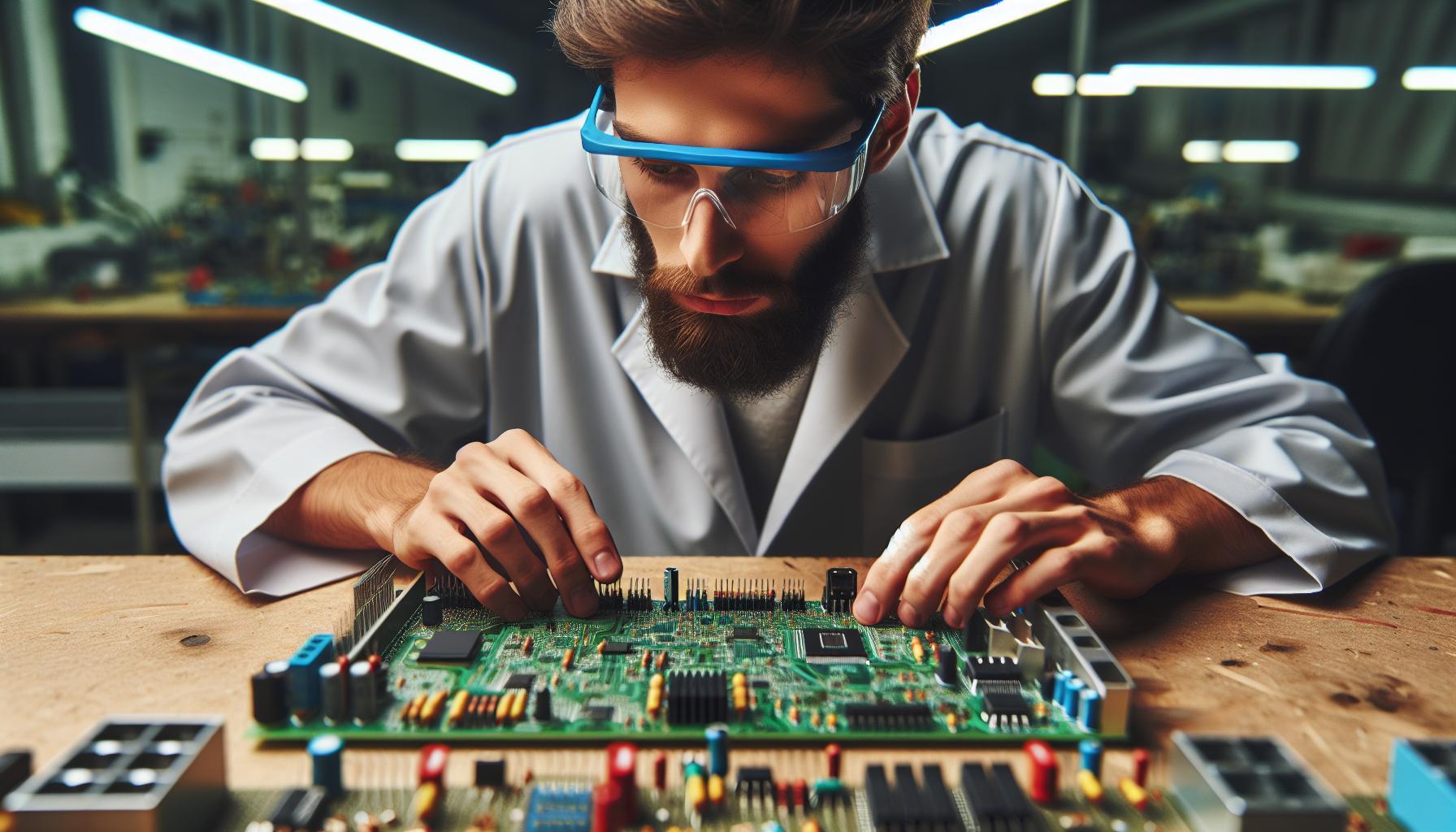
Assembling a PCB board can seem daunting, but it’s a rewarding process that opens the door to countless electronics projects. This guide breaks down the essential steps, from gathering materials to soldering components, ensuring even beginners can confidently create their own circuit boards. Understanding PCB assembly not only enhances technical knowledge but also empowers innovation in the constantly changing world of technology. Companies like WellPCB offer professional PCB assembly services to ensure high-quality production for both prototypes and large-scale manufacturing.
Tools And Materials Needed
Gathering the right tools and materials is crucial for assembling a PCB effectively. This section outlines essential tools and recommended materials for a successful project.
Essential Tools
- Soldering Iron: A reliable soldering iron allows for precise application of solder to components.
- Solder Wire: Use lead-free solder for a safer, environmentally friendly option.
- Wire Cutters: These are essential for trimming component leads after soldering.
- Tweezers: Fine-tipped tweezers assist in handling small components with accuracy.
- Multimeter: A multimeter measures voltage, current, and resistance, helping to verify circuit functionality.
- PCB Holder: A holder stabilizes the board, providing a steady platform for soldering.
- Magnifying Glass or Microscope: These tools help inspect solder joints and components for accuracy.
- Heat Shrink Tubing: This provides insulation for soldered connections and improves durability.
Recommended Materials
- PCB Blank: Choose a blank PCB that matches project specifications, such as size and layer count.
- Electronic Components: Gather all required components, including resistors, capacitors, and integrated circuits, according to the circuit schematic.
- Solder Paste: For surface-mounted components, solder paste facilitates even application of solder during the reflow process.
- Adhesive: Use a suitable adhesive for securing components that require additional stability.
- Gerber Files: Prepare Gerber files that specify each layer and component placement for manufacturing.
- Electrical Tape: This insulates exposed connections and provides protection against short circuits.
Understanding The PCB Layout
Understanding the PCB layout is crucial for successful assembly. A well-designed layout facilitates easier identification and placement of components, contributing to a more efficient assembly process.
Reading The Schematic
Reading the schematic involves interpreting symbols and connections on the diagram. Each symbol represents an electronic component, while lines indicate connections between them. He or she must recognize common symbols, such as resistors, capacitors, and integrated circuits. Familiarity with these symbols ensures accurate component placement on the board. Analyzing the schematic confirms correct pin configurations, verifying that components align with designated spots on the PCB.
Identifying Components
Identifying components requires careful examination of the schematic and the PCB layout. He or she should cross-reference the schematic with the component list, which details each part’s specifications, including type, value, and package size. Components often include passive elements like resistors and capacitors as well as active devices like transistors and ICs. Understanding these specifications aids in selecting the correct components before soldering. Familiarity with the physical appearance of components also simplifies the identification process during assembly, reducing errors.
Step-By-Step Assembly Process
Assembling a PCB involves several key steps to ensure accuracy and functionality. Each step contributes significantly to the overall success of the project.
Preparing The PCB
Prepare the PCB by cleaning its surface to remove dust and debris. Use isopropyl alcohol and a lint-free cloth for best results. Check for any discrepancies in the PCB layout, ensuring it aligns with the schematic. Verify that all necessary components and tools are available before starting the assembly. Make sure to have a stable work surface and good lighting to improve visibility.
Placing The Components
Place components according to the PCB layout. Start with smaller components, such as resistors and capacitors, before moving on to larger ones like connectors or integrated circuits. Insert components into their designated holes, ensuring they sit flat against the board. Use tweezers for precision, especially with tiny components. Cross-reference the placement with the schematic to avoid mistakes.
Soldering Techniques
Use a soldering iron for secure connections. Start by heating the pad on the PCB, then feed solder into the joint where the component lead meets the pad. Release the solder and remove the iron quickly to avoid excessive heat. Ensure clean and even solder joints for reliability. When working with surface-mounted components, apply solder paste before positioning the component, then reflow using a soldering method like hot air or a reflow oven. Regularly inspect solder joints for quality and connectivity.
Testing The Assembled PCB
Testing an assembled PCB ensures proper functionality and identifies any issues. Two primary testing methods include visual inspection and functional testing.
Visual Inspection
Visual inspection involves checking the PCB for obvious defects. Inspect for misplaced components, soldering errors, and signs of damage. Look for cold solder joints or bridges between neighboring pads. Use a magnifying glass or microscope to improve visibility during inspection. Conducting a thorough visual check can catch many issues before functional testing.
Functional Testing
Functional testing evaluates whether the assembled PCB operates as intended. Connect the PCB to a power source and observe its performance under normal operating conditions. Measure voltages at various points with a multimeter to ensure they align with schematic specifications. Utilize test equipment, like oscilloscopes or logic analyzers, to assess signal integrity and functionality. Identify any discrepancies and troubleshoot as needed. Functional testing confirms that the assembled PCB meets design requirements and operates reliably.
Common Mistakes To Avoid
Avoiding mistakes during PCB assembly enhances the overall quality and functionality of the circuit board. The following common pitfalls can lead to ineffective outcomes.
Overheating Components
Overheating components damages both the parts and the board. Most electronic components can tolerate specific temperature limits, exceeding these can lead to failure. Use a soldering iron with appropriate temperature control, typically around 350°C (662°F) for lead-free solder. Limit the time of contact to reduce heat exposure. Employ heat sinks on sensitive components to dissipate heat effectively during soldering and testing.
Incorrect Component Placement
Incorrect component placement often results in circuit failures. Each component must align precisely with its designated location on the PCB. Misplacement can cause short circuits or open connections. Refer to the schematic regularly to ensure accurate placement and orientation. Use a magnifying glass for better verification and arrange components systematically, starting from the smallest to largest for easier identification. Confirm pin connections match the design specifications before soldering to avoid irreversible errors.
Conclusion
Assembling a PCB board can be a rewarding experience that enhances both technical skills and creativity. By following the outlined steps and utilizing the right tools and materials, anyone can successfully create their own circuit board.
Attention to detail during the assembly process and thorough testing afterward are crucial for ensuring functionality. Avoiding common mistakes and maintaining a systematic approach will lead to better results and a deeper understanding of electronics.
With practice and persistence, the journey into PCB assembly can open doors to innovative projects and new opportunities in the tech world. Embracing this skill not only fosters personal growth but also contributes to advancements in technology.
Frequently Asked Questions
What is a PCB?
A Printed Circuit Board (PCB) is a flat board that electrically connects and supports electronic components. It is essential for organizing components in electronic devices.
What tools do I need for PCB assembly?
You’ll need a soldering iron, lead-free solder wire, wire cutters, fine-tipped tweezers, a multimeter, a PCB holder, a magnifying glass or microscope, and heat shrink tubing.
How do I prepare for PCB assembly?
Begin by cleaning the PCB surface and verifying the layout against the schematic. Gather all necessary materials and understand the placement of components.
What are the basic steps in PCB assembly?
The assembly process includes preparing the PCB, placing components in order, soldering connections, and inspecting solder joints to ensure quality.
How can I test my assembled PCB?
You can perform visual inspection to identify defects and conduct functional testing using a multimeter or oscilloscope to measure voltages and assess signal integrity.
What are common mistakes to avoid in PCB assembly?
Avoid overheating components, ensure correct placement of components according to the schematic, and regularly check your solder joints for quality and connectivity.
Why is understanding the PCB layout important?
Understanding the layout helps you accurately identify and place components, making the assembly process more efficient and reducing the likelihood of errors.
How can I improve my soldering technique?
Practice creating clean, even solder joints, use the right temperature settings on your soldering iron, and apply solder paste correctly for surface-mounted components.